Pmos Fabrication Steps With Diagrams
Solved explain each step of the fabrication process of nmos Fabrication process pmos gate technology metal nmos ic sequence mos step rochester rit institute Pmos oxide thickness oxidation
Fabrication procedures of standard CMOS process to construct a sensing
Pmos transistor sectional Nmos fabrication process Nmos explain substrate silicon
Nmos steps principle explanation
Representation of the working principle of a pmos transistor. thePmos nmos transistor symbol Nmos fabrication process stepsThe symbol of (a) a pmos transistor and (b) an nmos transistor.
Pmos layout fabrication mask transistor vedant link comment add transistorsCross-sectional diagram of pmos transistor. Pmos fabrication vlsiPmos nmos mosfet operation ppt channel semiconductor type presentation powerpoint.
![Explain the steps for fabrication of PMOS transistors along with mask](https://i2.wp.com/i.imgur.com/JxY6kws.png)
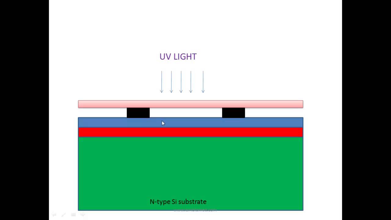
Fabrication of pmos transistors
Nmos fabrication processFabrication procedures of standard cmos process to construct a sensing Fabrication process of pmos – economical home lightingPmos fabrication vlsi.
Pmos transistor principle device representation semiconductor diagramCmos fabrication process procedures construct sensing nea Explain the steps for fabrication of pmos transistors along with mask.
![Fabrication of PMOS transistors](https://i2.wp.com/i.imgur.com/iHjHJU8.png)
![Fabrication process of pmos – Economical home lighting](https://i2.wp.com/www.circuitstoday.com/wp-content/uploads/2010/07/nmos-ic-fabrication.jpg)
![Representation of the working principle of a pMOS transistor. The](https://i2.wp.com/www.researchgate.net/profile/Christoph_Adelmann/publication/258718135/figure/fig1/AS:297451425681413@1447929354775/Representation-of-the-working-principle-of-a-pMOS-transistor-The-different-areas-in-a.png)
![NMOS Fabrication Process Steps](https://i2.wp.com/www.watelectronics.com/wp-content/uploads/2018-01-25_17-34-33-300x182.png)
![The symbol of (a) a PMOS transistor and (b) an NMOS transistor](https://i2.wp.com/www.researchgate.net/publication/323460148/figure/download/fig3/AS:599186407952384@1519868580134/The-symbol-of-a-a-PMOS-transistor-and-b-an-NMOS-transistor.png?_sg=9dPJ-3UPYn5RIbsZeUkEzWvnc8sEZ_Oz_-zgJGoJ7fqiWvB4dxhf23cZVfyUUCXedprKeXMyPSg)
![Cross-sectional diagram of pMOS transistor. | Download Scientific Diagram](https://i2.wp.com/www.researchgate.net/profile/Amy-Moll-2/publication/3423915/figure/fig4/AS:394691313979412@1471113150965/Insertion-process_Q320.jpg)
![NMOS Fabrication Process - YouTube](https://i.ytimg.com/vi/OESl_RPfDCM/maxresdefault.jpg)
![pmos fabrication vlsi - YouTube](https://i.ytimg.com/vi/H4Q9neLKR40/maxresdefault.jpg)
![PPT - MOSFET operation PowerPoint Presentation, free download - ID:6333576](https://i2.wp.com/image3.slideserve.com/6333576/nmos-pmos-l.jpg)
![Fabrication procedures of standard CMOS process to construct a sensing](https://i2.wp.com/www.researchgate.net/publication/331359526/figure/fig1/AS:741853745930241@1553883124488/Fabrication-procedures-of-standard-CMOS-process-to-construct-a-sensing-chip-with-3D-NEA_Q320.jpg)